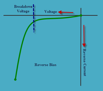
Testing Solar Panels V Vs I Curve Reverse Bias

I V Characteristic Of Pv Cell In Reverse Biased Region Download Scientific Diagram
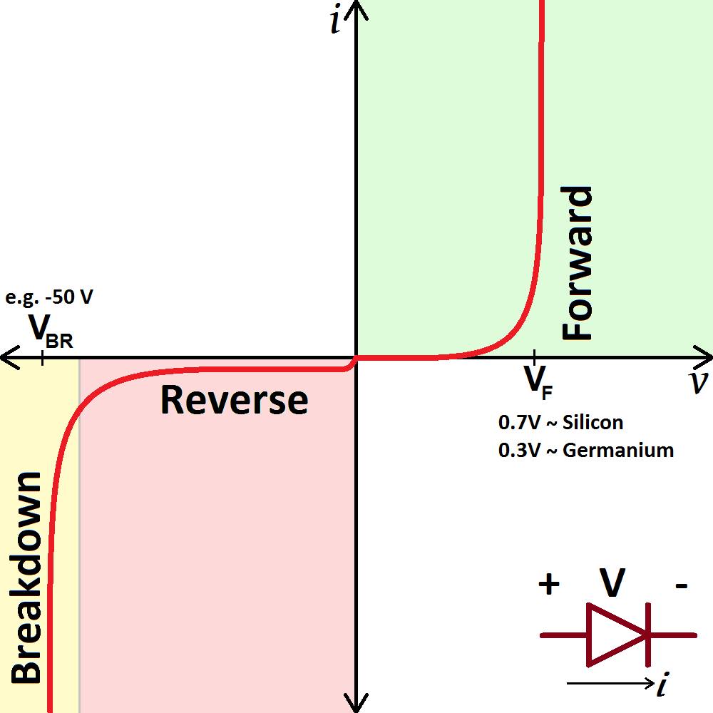
Diodes Learn Sparkfun Com

Pdf Reverse Bias Behavior Of Halide Perovskite Solar Cells

Zener Diode As Voltage Regulator Tutorial

Reverse Bias Behavior Of Halide Perovskite Solar Cells Bowring 2018 Advanced Energy Materials Wiley Online Library
Https Www Mdpi Com 1996 1073 11 9 2416 Pdf

Efficiency η efficiency is the ratio of the electrical power output p out compared to the solar power input p in into the pv cell.
Testing solar panels v vs i curve reverse bias.

V I Characteristics Of P N Junction Diode

I V Characteristic Curves Or Current Voltage Curves
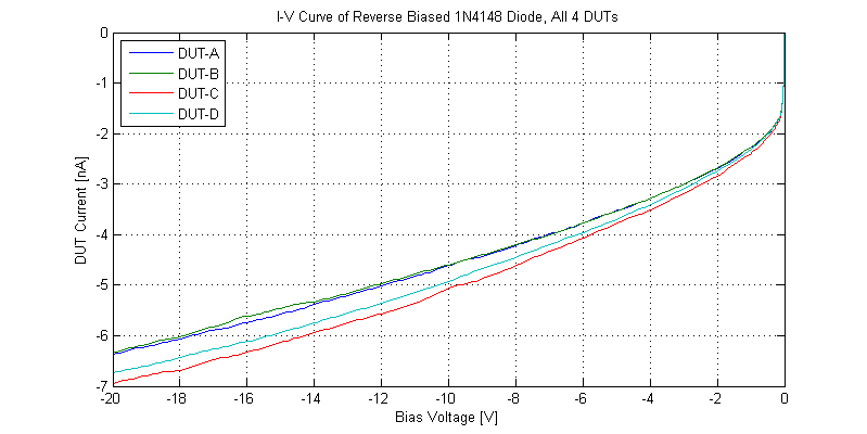
1n4148 Reverse Bias Leakage Current 2n3904blog

Schottky Diode Or Schottky Barrier Semiconductor Diode
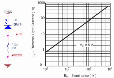
Measure Light Intensity Using Photodiode
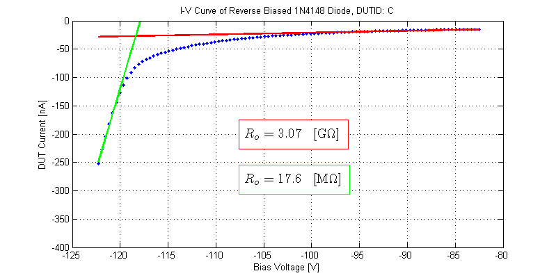
1n4148 Reverse Breakdown Voltage 2n3904blog

Pn Junction Diode Explained Forward Bias And Reverse Bias Youtube

To Draw The I V Characteristic Curve Of A P N Junction In Forward Bias And Reverse Bias Learn Cbse
P N Junction Diode Baising And Its Vi Characteristics
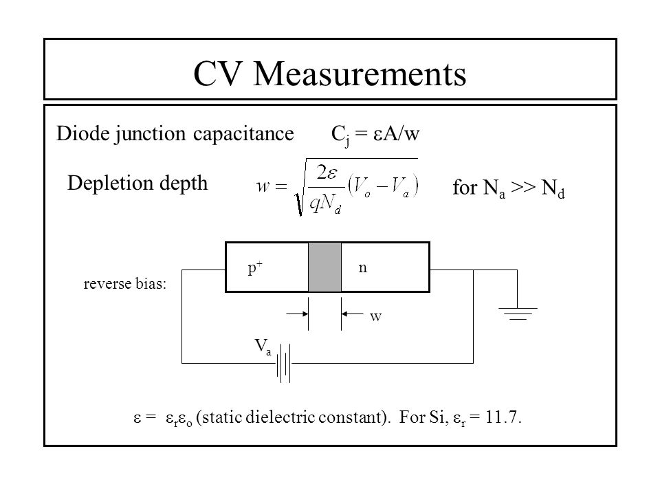
Cv Measurements Diode Junction Capacitance C J A W Depletion Depth Np P W Vava Reverse Bias R O Static Dielectric Constant For Si R Ppt Download

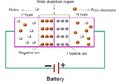
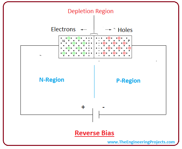
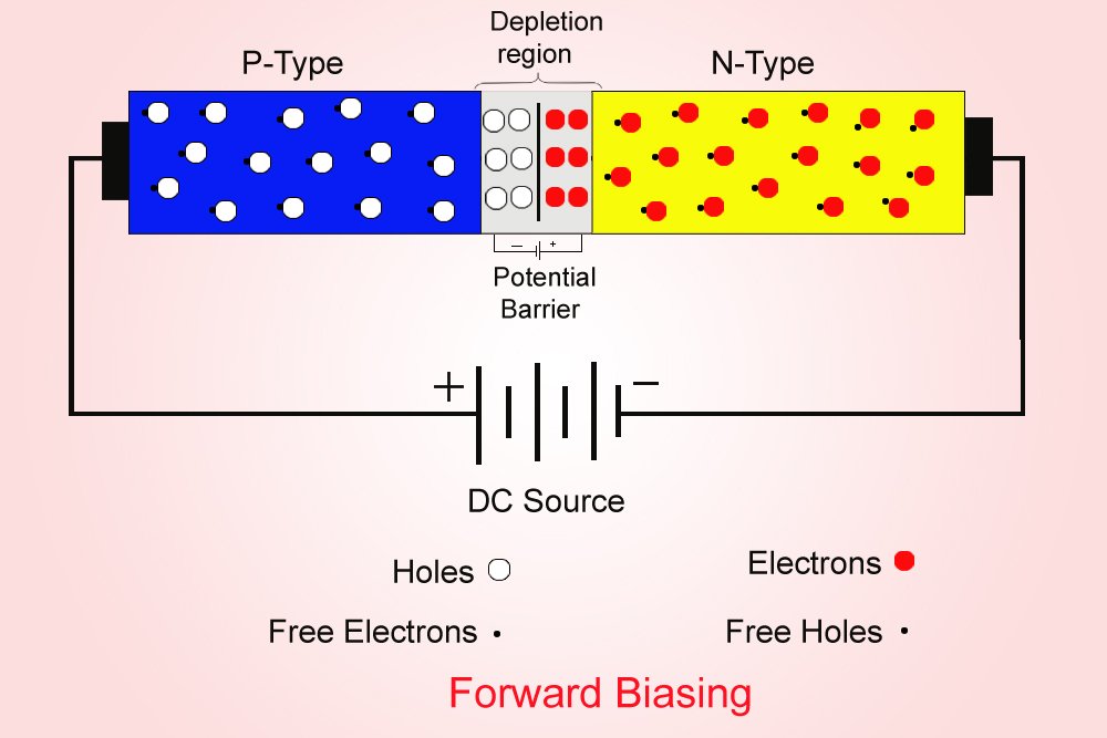
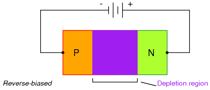
Forward Bias Reverse Bias Diode Working Animation Diode Depletion Region Reverse
Vi Characteristics Of Pn Junction Diode In 3 Biasing Modes
Introduction To Pn Junction The Engineering Projects

Rectifier What Is Rectifier Types Of Rectifier

Outline Chap 1 Introduction Chap 2 Basics Of Semiconductor Physics Ppt Video Online Download

Sensors Free Full Text P N Junction Photocurrent Modelling Evaluation Under Optical And Electrical Excitation Html

Pdf Effect Of Solar Cells Reverse Biased Voltage On Pv Modules Partial Shade Performance

Special Purpose P N Junction Diode Zener Diode Optoelectronic Devices
Https Encrypted Tbn0 Gstatic Com Images Q Tbn 3aand9gctav0nmpzhclr71hkuczehghcl6hu Vbux9xpac9khs1jfwmijr Usqp Cau
Zener Diode Definition Construction Working And Principles
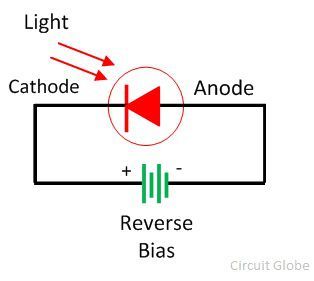
Difference Between Photodiode Phototransistor With Comparison Chart Circuit Globe

Diode Introduction Spinning Numbers
Lessons In Electric Circuits Volume Iii Semiconductors Chapter 3
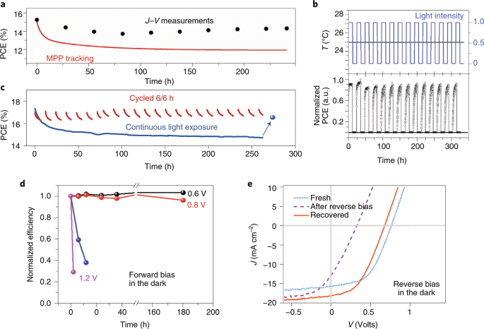
Consensus Statement For Stability Assessment And Reporting For Perovskite Photovoltaics Based On Isos Procedures Nature Energy
Source : pinterest.com
